반도체 웨이퍼 제조
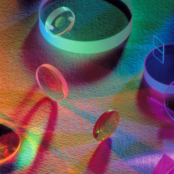
최첨단 광학, 레이저 및 복합 재료를 사용하여 처리량과 수율을 극대화하는 장비를 구축하십시오.
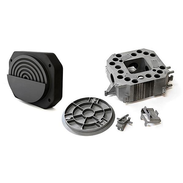
- 극도의 안정성열적으로 혁신적인 재료를 사용하여 리소그래피 및 웨이퍼 처리 도구를 구성하십시오.
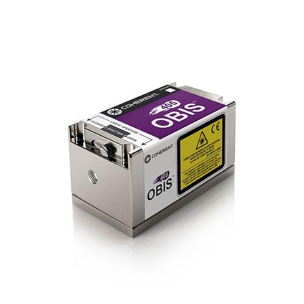
- 수율 증가거의 모든 검사 작업을 가능하게 하는 다양한 레이저 중에서 선택하십시오.
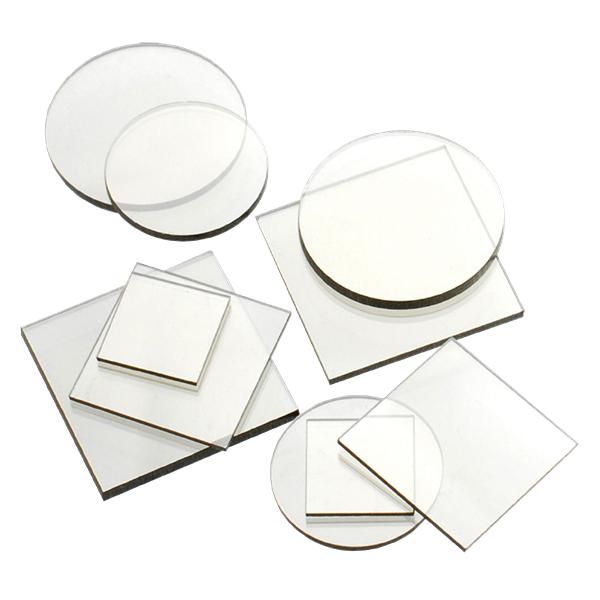
- 신뢰할 수 있는 EUV 리소그래피최고 품질의 CO2 레이저 광학 장치 및 다이아몬드 창으로 신뢰성과 수명을 보장합니다.


모든 노드에서의 성능
최첨단 3nm 칩부터 확립된 100nm+ 프로세스까지 바카라 카지노 레이저, 광학 및 고급 복합 재료로 도구를 구축하여 일관되고 비용 효율적이며 안정적인 작동을 보장하세요. 하이브리드 세라믹 및 탄화규소를 포함한 당사의 혁신적인 소재는 레이저 광학 및 다이아몬드 창과 마찬가지로 EUV 리소그래피의 극한 요구 사항을 충족하는 기계 부품을 생산합니다. 또한 당사의 전체 레이저 제품군은 거의 모든 검사 작업을 지원하고 마킹 및 어닐링과 같은 다양한 재료 가공 작업을 수행할 수 있습니다.

시작합시다
자신에 대한 정보를 제출해 주시면 제품 전문가가 영업일 기준 2일 이내에 연락을 드릴 것입니다.
제품 응용


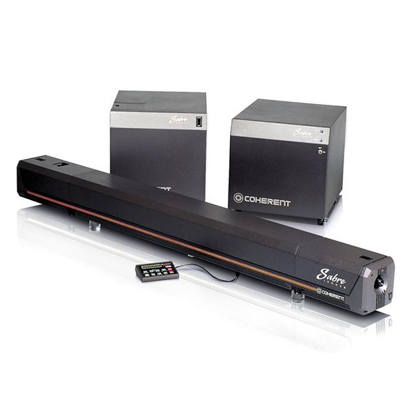
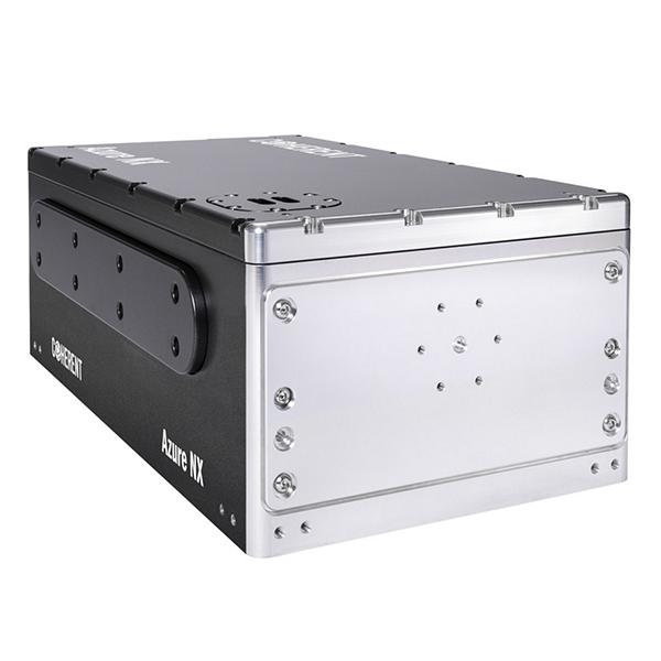
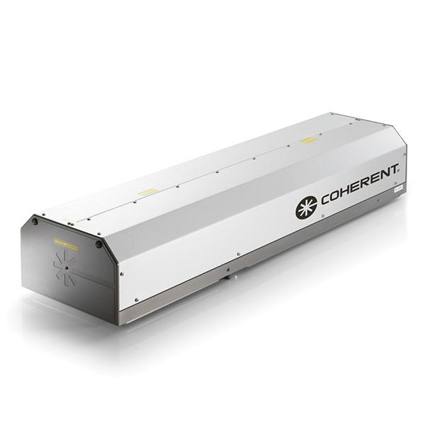
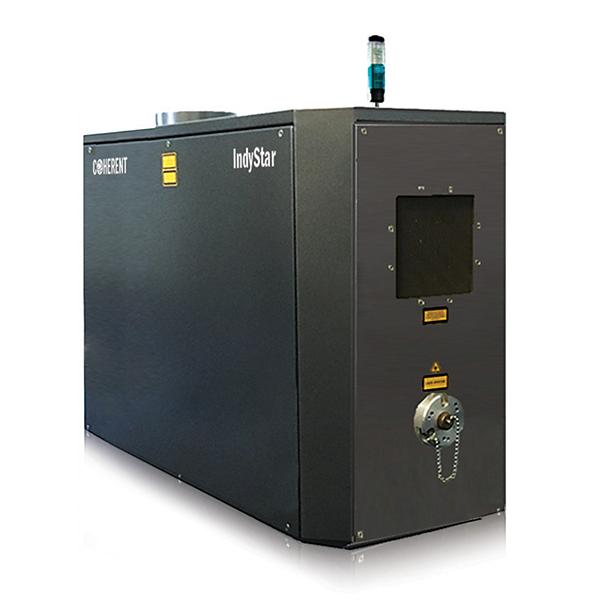
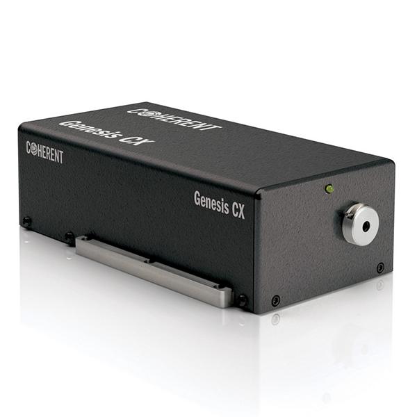
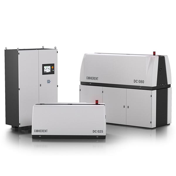
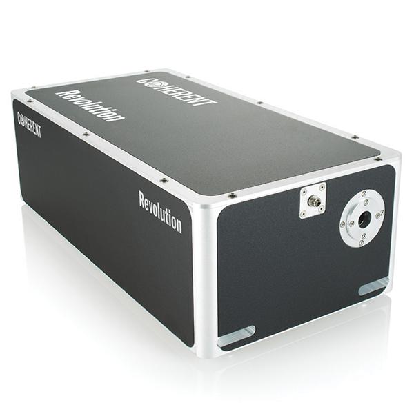
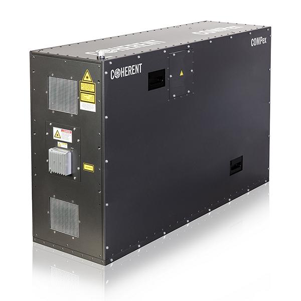
반도체 웨이퍼 제조 제품


바카라 카지노 쇼핑
바카라 카지노 온라인에서 레이저, 광섬유, 파워 미터 및 센서, 액세서리 등을 온라인 쇼핑하는 것이 그 어느 때보다 쉬워졌습니다.